Obstacle, cliff and gesture detection
64-zone ToF depth grid over a 45° field out to 4 m via i2c — obstacle, cliff and gesture detection.
Engineering inference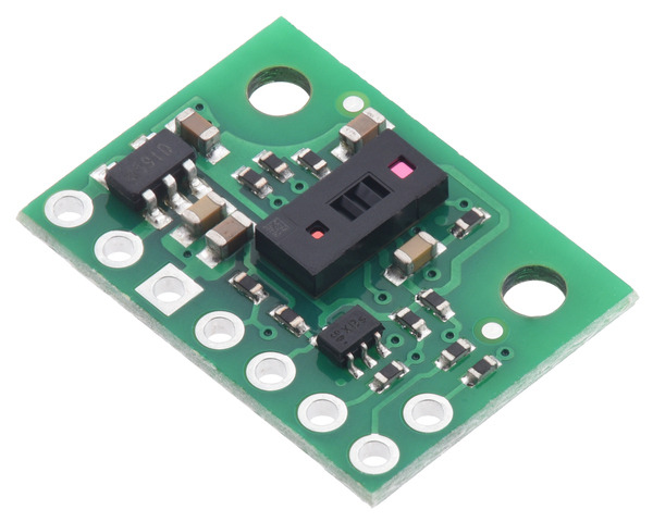
Pololu
Pololu 3417 carrier for the ST VL53L5CX multizone ToF sensor: 4×4 or 8×8 zones, 2–400 cm, 45° × 45° (63–65° diagonal) FoV, up to 60 Hz, 940 nm Class 1 VCSEL, I2C up to 1 MHz with level shifters, 2.5–5.5 V (3.3 V LDO), 100 mA typical, 13 × 18 × 3 mm, 0.5 g.
3417Development boardFacts about the complete product. Unknown values remain open design questions.
Guidance to help you shortlist. The basis is shown for each recommendation.
64-zone ToF depth grid over a 45° field out to 4 m via i2c — obstacle, cliff and gesture detection.
Engineering inferenceNo-load speed, rated performance and stall limits describe different operating points. A stall specification is not a continuous operating rating.
Generated from the datasheet's dimensioned drawing and measured against it. Download the STEP to check fit in your own enclosure.
How far it sees, how fast it scans, and how the robot reads it.
| Pin / wire | Position | Role | Notes |
|---|---|---|---|
| VDD | other | Regulated 3.3 V output . Up to around 100 mA is available to power external components. (If you want to bypass the internal regulator, you can instead use this pin as an input for voltages between 2.5 V and 3.6 V with VIN disconnected.) | |
| VIN | power in | This is the main 3.3 V to 5.5 V power supply connection. The SCL and SDA level shifters pull the I²C lines high to this level. | |
| GND | ground | The ground (0 V) connection for your power supply. Your I²C control source must also share a common ground with this board. | |
| SDA | i2c sda | Level-shifted I²C data line: HIGH is VIN, LOW is 0 V | |
| SCL | i2c scl | Level-shifted I²C clock line: HIGH is VIN, LOW is 0 V | |
| LPn | other | This pin is an active-low I²C disable input; the board pulls it up to VDD to enable I²C communication by default. Driving this pin low disables I²C communication (typically used as part of a process to change I²C addresses). This input is not level-shifted and it is not 5V-tolerant. | |
| INT | sync | Programmable interrupt output (VDD logic level). This output is not level-shifted. | |
| I2C_RST | other | This pin is an active-high I²C reset input; the board pulls it down to GND by default. Driving this pin high resets the I²C interface (but not the entire sensor). This input is not level-shifted and it is not 5V-tolerant. |
| Connector | Type |
|---|---|
| header | 8 × 0.1″ header holes: VDD, VIN, GND, SDA, SCL, LPn, INT, I2C_RST (headers included) |
Max range is the printed figure at the stated target reflectivity; accuracy is the typical datasheet value. Scan frequency is the default rotation or frame rate.
No-load, rated-load and stall figures retain their separate test conditions.
Stall torque and current are not continuous ratings. Check the duty cycle and starting load when choosing the driver and power supply.
Product operating conditions, chip ambient ratings, package case limits and junction maxima remain separate.
Reported product dimensions may exclude protruding components. Unknown height does not establish a complete clearance envelope.
Attached generated geometry is an approximate envelope. A generated outline does not establish an electrically verified PCB footprint.
| ID / type | Pins | Pitch | Notes |
|---|---|---|---|
| header8 × 0.1″ header holes: VDD, VIN, GND, SDA, SCL, LPn, INT, I2C_RST (headers included) | 8 | 2.54 mm | — |
Every available field, including details beyond the summaries. Null means the value has not been established.
US / USD is the target market. Observed price and stock are separate from a delivery quote.
US · USD
This observation is stale or has no verified check time. Recheck with the supplier.
Visit supplier (opens in a new tab)Delivery depends on quantity, postal code and shipping method. A dispatch statement such as “ship today” is not an arrival estimate.
Each source keeps its own verification status. Confirm the part revision and file contents before using it in a design.
Manufacturer reference
Manufacturer reference
inspected: green 0.5″ × 0.7″ carrier, black VL53L5CX module, 8 header holes, two mounting holes
Generated asset
cad_check passed
Generated envelope geometry may also exist for this record. It does not replace manufacturer CAD or a verified electrical land pattern.
Document provenance, retrieval dates and the field groups supported by each source.
Supports: spec.constraints.electrical.supply_voltage_max_v, spec.constraints.electrical.supply_voltage_min_v, spec.constraints.thermal.operating_temp_max_c, spec.constraints.thermal.operating_temp_min_c, spec.geometry.cad.bbox.height_mm, spec.geometry.cad.bbox.length_mm, spec.geometry.cad.bbox.width_mm, spec.geometry.cad.envelope_complete, spec.geometry.cad.mesh_path, spec.geometry.cad.step_path, spec.geometry.cad.verification, spec.geometry.dimensions.height_mm, spec.geometry.dimensions.length_mm, spec.geometry.dimensions.width_mm, spec.geometry.other.weight_g, spec.provides.accuracy_mm, spec.provides.accuracy_note, spec.provides.channels, spec.provides.features, spec.provides.fov_horizontal_deg, spec.provides.fov_vertical_deg, spec.provides.interface, spec.provides.laser_class, spec.provides.lidar_type, spec.provides.range_max_m, spec.provides.range_min_m, spec.provides.range_reflectivity_pct, spec.provides.ranging_method, spec.provides.ros2_driver, spec.provides.sample_rate_hz, spec.provides.scan_frequency_hz, spec.provides.wavelength_nm, spec.usage.connectors, spec.usage.pinout, spec.usage.pinout_complete, spec.usage.requirements.other.supply_current_ma
sha256 169ebe68ce93c3d9afeb7d0d06cb0626477a7236e6b1f1347e60c9aeebe3aa20
Supports: offers
Supply range 2.5–5.5 V.
From $19.95 at www.pololu.com. Prices are observed unit prices before tax and shipping.
18 × 13 × 3 mm. A STEP model is available for enclosure fit checks.
Every value in this record is traced to a source — 2 documents including the board and chip datasheets — with the page and table cited per value. Unknowns are left explicit, never guessed.