Camera and vision projects
Two 22-pin MIPI CSI camera connectors and up to 67 INT8 TOPS on a 1024-core Ampere GPU run multi-camera detection on the board.
Engineering inference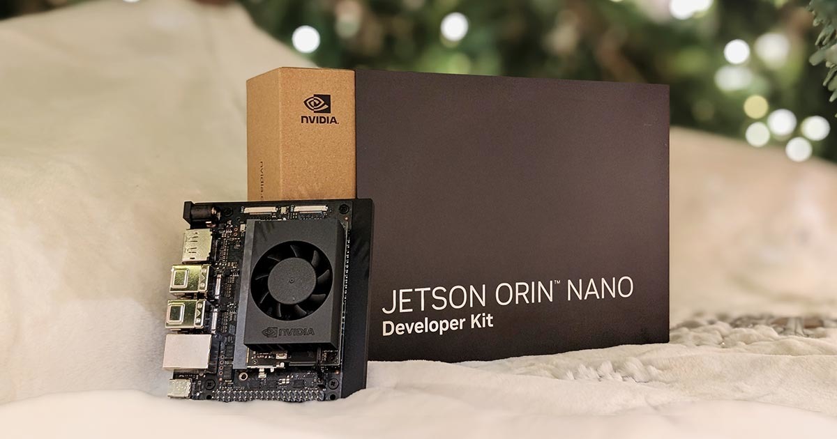
NVIDIA
NVIDIA Jetson Orin Nano Super Developer Kit: a 100 × 79 mm carrier with the 8 GB Orin Nano module, up to 67 INT8 TOPS, a 6-core Cortex-A78AE at 1.7 GHz and 102 GB/s LPDDR5 in 7–25 W modes. It has a 40-pin 3.3 V header (2× I2C, 2× SPI, UART, I2S), two 22-pin CSI camera connectors, two M.2 Key M slots, M.2 Key E, four USB 3.2 ports, DisplayPort and Gigabit Ethernet on a 9–20 V DC jack.
Jetson Orin Nano Super Developer KitRevision Carrier board spec SP-11324-001_v1.1Development boardFacts about the complete product. Unknown values remain open design questions.
Guidance to help you shortlist. The basis is shown for each recommendation.
Two 22-pin MIPI CSI camera connectors and up to 67 INT8 TOPS on a 1024-core Ampere GPU run multi-camera detection on the board.
Engineering inference67 INT8 TOPS, 32 Tensor cores and 8 GB LPDDR5 at 102 GB/s run neural networks locally instead of in the cloud.
Engineering inferenceSix Cortex-A78AE cores at 1.7 GHz, 8 GB LPDDR5 and NVMe storage on M.2 Key M host full Linux applications.
Engineering inferenceGigabit Ethernet RJ45 with an optional PoE header, four USB 3.2 ports and an optional CAN header connect it to wired robot and factory networks.
Engineering inferenceThe board is the parent product. Each chip has its own memory, pins, capabilities and thermal limits.
NVIDIA
78c54e2c-c5e7-5236-967b-cca663cae604--mcuGenerated from the datasheet's dimensioned drawing and measured against it. Download the STEP to check fit in your own enclosure.
40 board pins and 28 explicit routes documented. The record marks the pinout complete. Alternate functions can share pins and may not be usable together.
Board connector positions are the physical points you wire to.
| Board pin | Connector / position | Electrical | Functions / constraints |
|---|---|---|---|
| 3.3VID J12-1 | J12Position 1 | power out | power_out |
| 5.0VID J12-2 | J12Position 2 | power out | power_out |
| I2C1_SDAID J12-3 | J12Position 3 | gpio5 V tolerant: noMax drive 2 mA | I2C1_SDA, I2C #1 Data |
| 5.0VID J12-4 | J12Position 4 | power out | power_out |
| I2C1_SCLID J12-5 | J12Position 5 | gpio5 V tolerant: noMax drive 2 mA | I2C1_SCL, I2C #1 Clock |
| GNDID J12-6 | J12Position 6 | 0 Vground | ground |
| GPIO09ID J12-7 | J12Position 7 | gpioMax drive 20 mA | GPIO09, Audio Primary Clock |
| UART1_TXDID J12-8 | J12Position 8 | gpioMax drive 20 mA | UART1_TXD, UART #1 Transmit |
| GNDID J12-9 | J12Position 9 | 0 Vground | ground |
| UART1_RXDID J12-10 | J12Position 10 | gpioMax drive 20 mA | UART1_RXD, UART #1 Receive |
| UART1_RTS*ID J12-11 | J12Position 11 | gpioMax drive 20 mA | UART1_RTS*, UART #2 Request to Send |
| I2S0_SCLKID J12-12 | J12Position 12 | gpioMax drive 20 mA | I2S0_SCLK, Audio I2S #0 Clock |
| SPI1_SCKID J12-13 | J12Position 13 | gpioMax drive 20 mA | SPI1_SCK, SPI #1 Shift Clock |
| GNDID J12-14 | J12Position 14 | 0 Vground | ground |
| GPIO12ID J12-15 | J12Position 15 | gpioMax drive 20 mA | GPIO12 |
| SPI1_CSI1*ID J12-16 | J12Position 16 | gpioMax drive 20 mA | SPI1_CSI1*, SPI #1 Chip Select #1 Bidir/Output |
| 3.3VID J12-17 | J12Position 17 | power out | power_out |
| SPI1_CSI0*ID J12-18 | J12Position 18 | gpioMax drive 20 mA | SPI1_CSI0*, SPI #0 Chip Select #0 Bidir/Output |
| SPI0_MOSIID J12-19 | J12Position 19 | gpioMax drive 20 mA | SPI0_MOSI, SPI #0 Primary Out/Secondary In |
| GNDID J12-20 | J12Position 20 | 0 Vground | ground |
| SPI0_MISOID J12-21 | J12Position 21 | gpioMax drive 20 mA | SPI0_MISO, SPI #0 Primary In/Secondary Out |
| SPI1_MISOID J12-22 | J12Position 22 | gpioMax drive 20 mA | SPI1_MISO, SPI #1 Primary In/Secondary Out |
| SPI0_SCKID J12-23 | J12Position 23 | gpioMax drive 20 mA | SPI0_SCK, SPI #0 Shift Clock |
| SPI0_CS0*ID J12-24 | J12Position 24 | gpioMax drive 20 mA | SPI0_CS0*, SPI #0 Chip Select #0 Bidir/Output |
| GNDID J12-25 | J12Position 25 | 0 Vground | ground |
| SPI0_CS1*ID J12-26 | J12Position 26 | gpioMax drive 20 mA | SPI0_CS1*, SPI #0 Chip Select #1 Bidir/Output |
| I2C0_SDAID J12-27 | J12Position 27 | gpio5 V tolerant: noMax drive 2 mA | I2C0_SDA, I2C #0 Data |
| I2C0_SCLID J12-28 | J12Position 28 | gpio5 V tolerant: noMax drive 2 mA | I2C0_SCL, I2C #0 Clock |
| GPIO01ID J12-29 | J12Position 29 | gpioMax drive 20 mA | GPIO01, General Purpose Clock #0 |
| GNDID J12-30 | J12Position 30 | 0 Vground | ground |
| GPIO11ID J12-31 | J12Position 31 | gpioMax drive 20 mA | GPIO11, General Purpose Clock #1 |
| GPIO07ID J12-32 | J12Position 32 | gpioMax drive 20 mA | GPIO07, PWM |
| GPIO13ID J12-33 | J12Position 33 | gpioMax drive 20 mA | GPIO13, PWM |
| GNDID J12-34 | J12Position 34 | 0 Vground | ground |
| I2S0_FSID J12-35 | J12Position 35 | gpioMax drive 20 mA | I2S0_FS, Audio I2S #0 Field Select |
| UART1_CTS*ID J12-36 | J12Position 36 | gpioMax drive 20 mA | UART1_CTS*, UART #1 Clear to Send |
| SPI1_MOSIID J12-37 | J12Position 37 | gpioMax drive 20 mA | SPI1_MOSI, SPI #1 Primary Out/Secondary In |
| I2S0_DINID J12-38 | J12Position 38 | gpioMax drive 20 mA | I2S0_DIN, Audio I2S #0 Data in |
| GNDID J12-39 | J12Position 39 | 0 Vground | ground |
| I2S0_DOUTID J12-40 | J12Position 40 | gpioMax drive 20 mA | I2S0_DOUT, Audio I2S #0 Data Out |
A board label, a chip signal ID and a package lead number are different identifiers.
| Board connection | Chip instance | Chip signal | Package lead | Route |
|---|---|---|---|---|
J12-3 | Jetson Orin Nano 8GBInstance 78c54e2c-c5e7-5236-967b-cca663cae604--mcu | I2C1_SDAID I2C1_SDA | — | direct |
J12-5 | Jetson Orin Nano 8GBInstance 78c54e2c-c5e7-5236-967b-cca663cae604--mcu | I2C1_SCLID I2C1_SCL | — | direct |
J12-7 | Jetson Orin Nano 8GBInstance 78c54e2c-c5e7-5236-967b-cca663cae604--mcu | GPIO09ID GPIO09 | — | level shifted |
J12-8 | Jetson Orin Nano 8GBInstance 78c54e2c-c5e7-5236-967b-cca663cae604--mcu | UART1_TXDID UART1_TXD | — | level shifted |
J12-10 | Jetson Orin Nano 8GBInstance 78c54e2c-c5e7-5236-967b-cca663cae604--mcu | UART1_RXDID UART1_RXD | — | level shifted |
J12-11 | Jetson Orin Nano 8GBInstance 78c54e2c-c5e7-5236-967b-cca663cae604--mcu | UART1_RTS*ID UART1_RTS* | — | level shifted |
J12-12 | Jetson Orin Nano 8GBInstance 78c54e2c-c5e7-5236-967b-cca663cae604--mcu | I2S0_SCLKID I2S0_SCLK | — | level shifted |
J12-13 | Jetson Orin Nano 8GBInstance 78c54e2c-c5e7-5236-967b-cca663cae604--mcu | SPI1_SCKID SPI1_SCK | — | level shifted |
J12-15 | Jetson Orin Nano 8GBInstance 78c54e2c-c5e7-5236-967b-cca663cae604--mcu | GPIO12ID GPIO12 | — | level shifted |
J12-16 | Jetson Orin Nano 8GBInstance 78c54e2c-c5e7-5236-967b-cca663cae604--mcu | SPI1_CS1*ID SPI1_CS1* | — | level shifted |
J12-18 | Jetson Orin Nano 8GBInstance 78c54e2c-c5e7-5236-967b-cca663cae604--mcu | SPI1_CS0*ID SPI1_CS0* | — | level shifted |
J12-19 | Jetson Orin Nano 8GBInstance 78c54e2c-c5e7-5236-967b-cca663cae604--mcu | SPI0_MOSIID SPI0_MOSI | — | level shifted |
J12-21 | Jetson Orin Nano 8GBInstance 78c54e2c-c5e7-5236-967b-cca663cae604--mcu | SPI0_MISOID SPI0_MISO | — | level shifted |
J12-22 | Jetson Orin Nano 8GBInstance 78c54e2c-c5e7-5236-967b-cca663cae604--mcu | SPI1_MISOID SPI1_MISO | — | level shifted |
J12-23 | Jetson Orin Nano 8GBInstance 78c54e2c-c5e7-5236-967b-cca663cae604--mcu | SPI0_SCKID SPI0_SCK | — | level shifted |
J12-24 | Jetson Orin Nano 8GBInstance 78c54e2c-c5e7-5236-967b-cca663cae604--mcu | SPI0_CS0*ID SPI0_CS0* | — | level shifted |
J12-26 | Jetson Orin Nano 8GBInstance 78c54e2c-c5e7-5236-967b-cca663cae604--mcu | SPI0_CS1*ID SPI0_CS1* | — | level shifted |
J12-27 | Jetson Orin Nano 8GBInstance 78c54e2c-c5e7-5236-967b-cca663cae604--mcu | I2C0_SDAID I2C0_SDA | — | direct |
J12-28 | Jetson Orin Nano 8GBInstance 78c54e2c-c5e7-5236-967b-cca663cae604--mcu | I2C0_SCLID I2C0_SCL | — | direct |
J12-29 | Jetson Orin Nano 8GBInstance 78c54e2c-c5e7-5236-967b-cca663cae604--mcu | GPIO01ID GPIO01 | — | level shifted |
J12-31 | Jetson Orin Nano 8GBInstance 78c54e2c-c5e7-5236-967b-cca663cae604--mcu | GPIO11ID GPIO11 | — | level shifted |
J12-32 | Jetson Orin Nano 8GBInstance 78c54e2c-c5e7-5236-967b-cca663cae604--mcu | GPIO07ID GPIO07 | — | level shifted |
J12-33 | Jetson Orin Nano 8GBInstance 78c54e2c-c5e7-5236-967b-cca663cae604--mcu | GPIO13ID GPIO13 | — | level shifted |
J12-35 | Jetson Orin Nano 8GBInstance 78c54e2c-c5e7-5236-967b-cca663cae604--mcu | I2S0_FSID I2S0_FS | — | level shifted |
J12-36 | Jetson Orin Nano 8GBInstance 78c54e2c-c5e7-5236-967b-cca663cae604--mcu | UART1_CTS*ID UART1_CTS* | — | level shifted |
J12-37 | Jetson Orin Nano 8GBInstance 78c54e2c-c5e7-5236-967b-cca663cae604--mcu | SPI1_MOSIID SPI1_MOSI | — | level shifted |
J12-38 | Jetson Orin Nano 8GBInstance 78c54e2c-c5e7-5236-967b-cca663cae604--mcu | I2S0_DINID I2S0_DIN | — | level shifted |
J12-40 | Jetson Orin Nano 8GBInstance 78c54e2c-c5e7-5236-967b-cca663cae604--mcu | I2S0_DOUTID I2S0_DOUT | — | level shifted |
Chip signals stay attached to their chip instance, including their package lead and board exposure.
Chip package pins have not been transcribed for this instance.
Supply voltage and GPIO logic voltage describe different parts of the design.
A 5 V supply input does not establish 5 V tolerance on GPIO. Check the documented power input and logic domain for each connection.
These describe the assembled board. Interface counts do not guarantee simultaneous operation.
| Interface | Support | Count | Details |
|---|---|---|---|
| gpio | Documented | Unknown | J12-3, J12-5, J12-7, J12-8, J12-10, J12-11, J12-12, J12-13, J12-15, J12-16, J12-18, J12-19, J12-21, J12-22, J12-23, J12-24, J12-26, J12-27, J12-28, J12-29, J12-31, J12-32, J12-33, J12-35, J12-36, J12-37, J12-38, J12-40 |
| i2c | Documented | Unknown | J12-3, J12-5, J12-27, J12-28 |
| clock | Documented | Unknown | J12-7, J12-29, J12-31 |
| uart | Documented | Unknown | J12-8, J12-10, J12-11, J12-36 |
| i2s | Documented | Unknown | J12-12, J12-35, J12-38, J12-40 |
| spi | Documented | Unknown | J12-13, J12-16, J12-18, J12-19, J12-21, J12-22, J12-23, J12-24, J12-26, J12-37 |
| pwm | Documented | Unknown | J12-32, J12-33 |
Board capacity includes installed memory; chip-local memory is listed separately under each processor.
Capacities use KiB / MiB (1024-based units). Firmware partitions and runtime allocations reduce application-available memory.
Product operating conditions, chip ambient ratings, package case limits and junction maxima remain separate.
Reported product dimensions may exclude protruding components. Unknown height does not establish a complete clearance envelope.
Attached generated geometry is an approximate envelope. A generated outline does not establish an electrically verified PCB footprint.
| ID / type | Pins | Pitch | Notes |
|---|---|---|---|
| J122x20 40-pin expansion header, 2.54 mm pitch | 40 | 2.54 mm | — |
| J2022-position MIPI CSI camera connector (camera 0) | Unknown | Unknown | — |
| J2122-position MIPI CSI camera connector (camera 1) | Unknown | Unknown | — |
| J10M.2 Key E slot | Unknown | Unknown | — |
| J11M.2 Key M slot, PCIe Gen3 x4 | Unknown | Unknown | — |
| J24M.2 Key M slot, PCIe Gen3 x2 | Unknown | Unknown | — |
| J8DisplayPort | Unknown | Unknown | — |
| J15Gigabit Ethernet RJ45 | Unknown | Unknown | — |
| J5USB Type-C (recovery mode) | Unknown | Unknown | — |
| J6USB 3.2 Type-A x2 | Unknown | Unknown | — |
| J7USB 3.2 Type-A x2 | Unknown | Unknown | — |
| J1412-pin button header (power, reset, recovery, debug UART) | Unknown | Unknown | — |
| J17optional CAN header | Unknown | Unknown | — |
| J13fan connector (5 V, PWM, tach) | Unknown | Unknown | — |
| J16DC power jack, 9-20 V | Unknown | Unknown | — |
Every available field, including details beyond the summaries. Null means the value has not been established.
US / USD is the target market. Observed price and stock are separate from a delivery quote.
US · USD
This observation is stale or has no verified check time. Recheck with the supplier.
Visit supplier (opens in a new tab)Delivery depends on quantity, postal code and shipping method. A dispatch statement such as “ship today” is not an arrival estimate.
Each source keeps its own verification status. Confirm the part revision and file contents before using it in a design.
Manufacturer reference
Manufacturer reference
inspected: Jetson Orin Nano developer kit carrier board with the module, black heatsink and fan, next to its retail box
Generated asset
cad_check passed
Generated envelope geometry may also exist for this record. It does not replace manufacturer CAD or a verified electrical land pattern.
Document provenance, retrieval dates and the field groups supported by each source.
Supports: spec.constraints.electrical.io_voltage_v, spec.constraints.electrical.logic_high_min_v, spec.constraints.electrical.max_current_ma, spec.constraints.electrical.pin_drive_max_ma, spec.constraints.electrical.supply_voltage_max_v, spec.constraints.electrical.supply_voltage_min_v, spec.constraints.electrical.supply_voltage_nominal_v, spec.constraints.thermal.operating_temp_max_c, spec.constraints.thermal.operating_temp_min_c, spec.geometry.cad.bbox.height_mm, spec.geometry.cad.bbox.length_mm, spec.geometry.cad.bbox.width_mm, spec.geometry.cad.envelope_complete, spec.geometry.cad.mesh_path, spec.geometry.cad.step_path, spec.geometry.cad.verification, spec.geometry.dimensions.height_mm, spec.geometry.dimensions.length_mm, spec.geometry.dimensions.width_mm, spec.provides.capabilities, spec.provides.features, spec.provides.gpio_count, spec.provides.memory.sram_kb, spec.provides.software_frameworks, spec.usage.connectors, spec.usage.pin_mappings, spec.usage.pinout, spec.usage.pinout_complete
sha256 fb8fc00fdb7effdcb176c5e5663f5b1a8ace09e2f35ed679c3672d4589d335f7
Supports: offers
The NVIDIA Jetson Orin Nano Super Dev Kit is built around the Jetson Orin Nano 8GB.
28 GPIO pins are exposed. Xirkit documents 40 board pins, 28 of them with pin-level electrical limits.
No. The I/O pins are not 5 V tolerant — they run at 3.3 V logic; use a level shifter for 5 V signals. Input-high threshold: 2.64–3.63 V.
Documented output-high current per pin: ≤ 20 uA. Values are traced to the chip datasheet; see the pinout table for per-pin limits and conditions.
Supply range 19–19 V.
From $399 at www.sparkfun.com. Prices are observed unit prices before tax and shipping.
100 × 79 × 1.57 mm. A STEP model is available for enclosure fit checks.
gpio, i2c, clock, uart, i2s, spi, pwm.
Supported frameworks: NVIDIA Jetson Linux, CUDA.
Every value in this record is traced to a source — 2 documents including the board and chip datasheets — with the page and table cited per value. Unknowns are left explicit, never guessed.